EVGA X99 FTW K Motherboard Review
Author: Dennis GarciaEnthusiast Features
Benchtop controls are located in the upper right of the motherboard near the 24 pin power connector and consist of power, reset and CMOS clear. Nearby you'll find the dual purpose debug LED that reads off post codes during boot and later relays CPU temp.
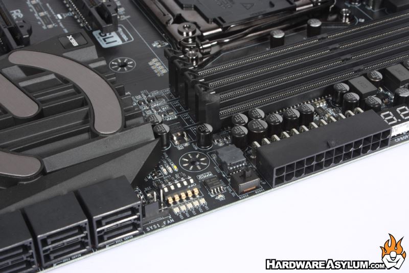
Voltage test points are no longer a series of pads on the PCB but are instead consist of meter friendly test leads located in a pin block behind the memory slots. Test leads are included and follow the standard format found on similar EVGA video cards.
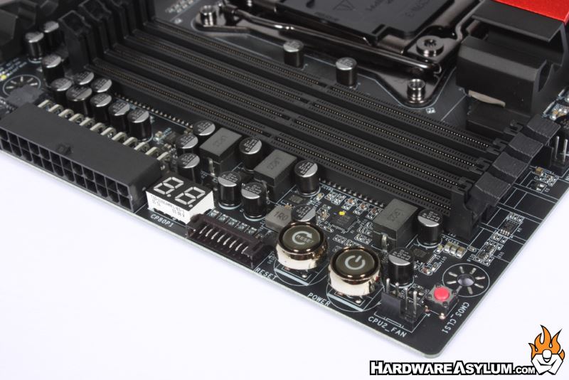
The X99 FTW K comes with a dual BIOS with the selector switch located next to the 24-pin power connector and a red LED will indicate which BIOS chip is currently active. A single BIOS chip is replaceable and located near the onboard PCI Express disable switches.
Above the SATA connections you will find a series of jumpers which allow you to disable any of the PCI Express slots for debugging. It also gives you a convenient way to run multi card benchmarks without having to tear everything down. A new feature is an indicator light next to the switch indicating what PCI Express slot is populated and how fast the connection is.
M.2 slots have become a popular addition on all motherboards giving system builders the option of customizing their motherboard installation without sacrificing any of the PCI Express slots. For instance installing a wireless AC card would normally take up a single PCI Express slot however dropping one into a M.2 Type 2 enables wireless connectivity while still allowing you room for 4-way SLI.
Err, 3-way SLI. If this expansion is populated it will disable PCI Express slot PE6 or the seventh slot on the motherboard.
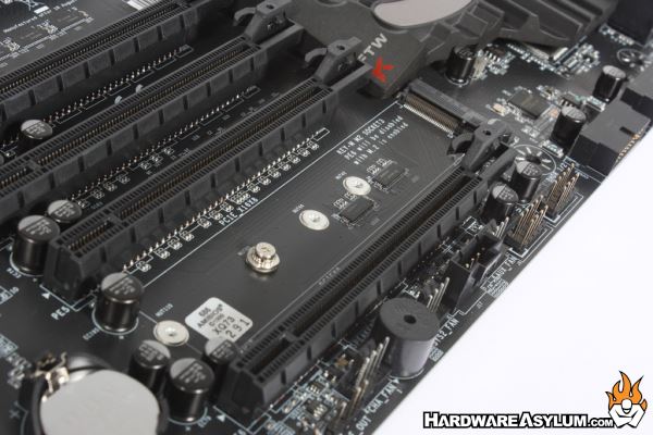
The EVGA X99 FTW K comes with a single M Key M.2 port and supports four different sizes up to 110mm.