EVGA X99 FTW K Motherboard Review
Author: Dennis GarciaBoard Layout and Features
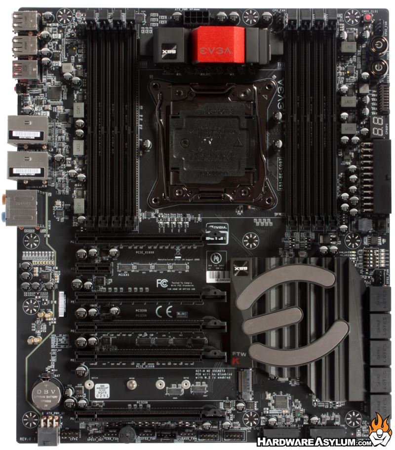
Some of the most popular EVGA motherboards followed a classic color scheme featuring a jet black PCB and red expansion slots. Well, the X99 FTW featured that color scheme which has been completely blacked out including the EVGA “E” on the heatsink. In fact, the only red on the entire motherboard is a small section of the VRM heatsink.
The PCB features a respectable 8 layer design which helps prevent the board from flexing under stress and improves signal integrity.
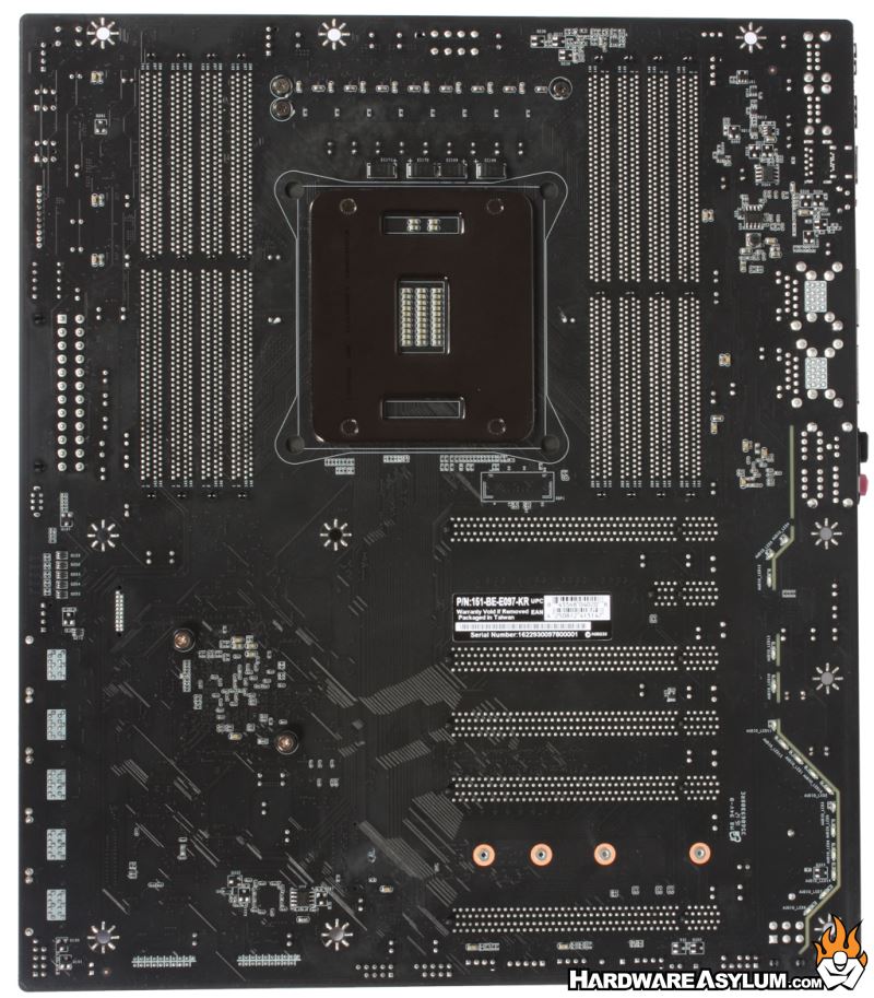
Flipping the motherboard over can tell you a lot about how it is constructed including where some of the major chips are located and slot layout. Every PCI Express slot is fully wired meaning that the full slot width is soldered to the PCB. That doesn't always mean each slot comes with full set of PCI Express lanes but does simplify the board design a little.
EVGA has chosen a traditional VRM design that places all of the power phases above the processor socket between the memory banks. Keeping the VRM cool is an important aspect of overclocking and EVGA has included a large ornate heatsink that covers the entire 8-phase VRM.
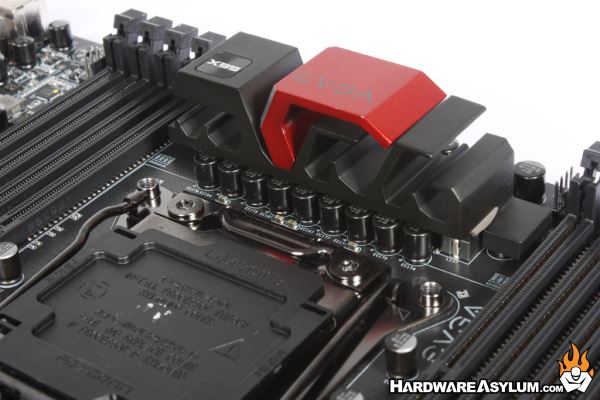
LN2 insulation could be tricky given the proximity between CPU socket and everything else, just make sure to take your time and cover the gaps.
Moving towards the CPU socket we can see that EVGA went with a typical heatsink retention system with the threaded holes on top of the PCB and attached to the CPU socket. These CPU sockets are quite strong so there is very little chance you’ll bend one. That is unless you are really trying or happen to drop your motherboard with a CPU pot attached.
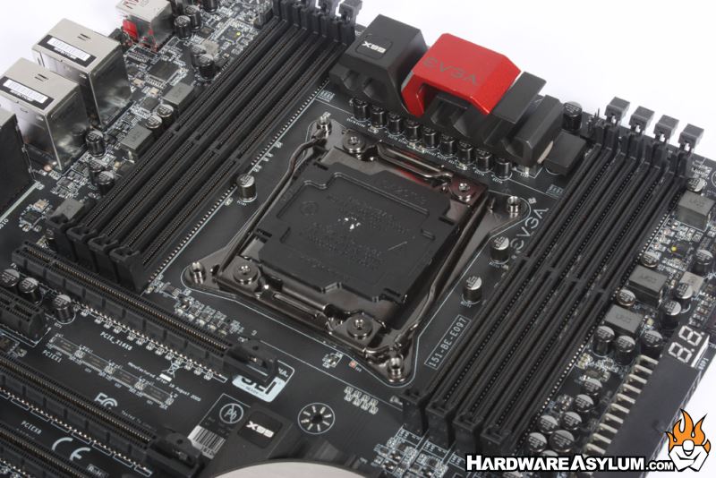
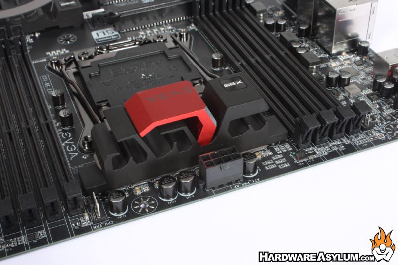
CPU Power is provided by a single 8-pin power connector located behind the VRM cooler.