EVGA Z87 Classified Motherboard Review
Author: Dennis GarciaEnthusiast Features
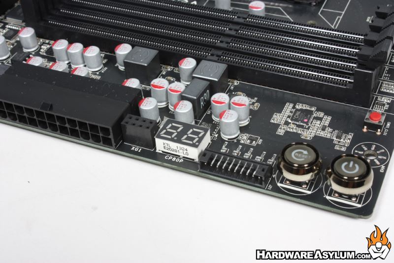
Benchtop controls are located in the upper left of the motherboard near the 24 pin power connector and consist of power, reset and CMOS clear. Nearby you'll find a dual purpose debug LED that reads off post codes during boot and later relays CPU temp. Below the debug LED is a fairly new onboard feature called GPU Link. There is very little documentation related to this set of plugs but, we have determined that the feature is currently only supported on the EVGA GTX 580. When active it allows you to control the GPU through the motherboard UEFI.
Let’s hope this feature is expanded on in the future.
Voltage test points are no longer a series of pads on the PCB but instead can be found as a pin block located near the power and reset switches. The test leads that connect here are voltage meter friendly and follow a standard format found on custom EVGA video cards.
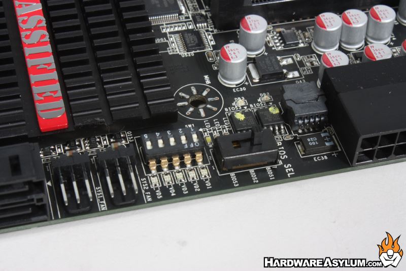
Above the SATA connections you will find a series of DIP switches which allow you to disable any of the PCI Express slots. This gives you a convenient way to run multi card benchmarks without having to tear everything down and also helps you debug when something goes wrong. Next to these you’ll find the BIOS selection switch for enabling one of the three onboard BIOS chips.
You may also notice that one of the chips is removable allowing you a bootable option in case of a triple BIOS failure or when you need access to more than three images.
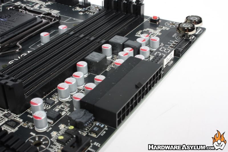
One of the most revolutionary advances in motherboard construction was the advent of 90 degree IDE/SATA connections. By positioning them parallel to the motherboard you can get cleaner cable routes and improve overall airflow. EVGA has started positioning all of their major cables parallel to the motherboard including the 24pin main power, fan headers and onboard PCI Express power.